我在本课程中设计的主要原理图块是项目框图、“功率预算框图”、“RK3399 的电源原理图”、“RK3399 的 PMUIO 原理图块”、“RK3399 的 EMMC/PCIE/ADC 原理图”、“ RK3399 的 EDP/MIPI-DSI/HDMI 原理图,“RK3399 的 Type-C/USB3.0/USB2.0 主机原理图”,“RK3399 的 MIPI-CSI/GPIOs/I2C 原理图”,“MII/RMII/GMII/ RK3399 的 RGMII 原理图”、“RK3399 的 SDR/DDRx/LPDDRx 原理图”、“RK3399 的 PMIC/DC-DC/LDO/降压-升压”以及您将在本课程中学习的更多各种子部分,如您在课程中所见部分。
您还将学习一些基本的硬件设计模块,例如您还将学习一些基本模块:
预原理图设计块(框图和功率预算)
层堆叠选择和定义任何堆叠的规则
不同的接地技术(信号接地、大地接地、机箱接地)
任何 PCB 的配电网络分析(PDN 分析)。
还有更多的东西。
铁氧体磁珠、ESD 二极管和磁性应用及其选择。
如何在 Microsoft-Paint 上进行布局和布局规划等等。
完成本课程后,您可以在没有任何仿真模型和第三方支持的情况下设计任何“处理器板”。
课程目录
我已将本课程分为 #13 个不同的部分,每个部分下您会发现多个课程:
第 1 部分:非常详细地讨论要求表和处理器 RK3399 数据表。
第 2 部分:如何选择 SDRAM (SDR/DDRX/LPDDRX)?从头开始,其引脚映射和原理图设计来自数据表。
第 3 节:详细介绍 PMIC(电源管理 IC)的选择和原理图设计。
第 4 部分:EMMC(嵌入式多媒体卡)芯片选择、引脚映射和原理图设计。
第 5 部分:WIFI/BT 模块选择、认证(美国/欧盟/加拿大)、选择和原理图设计。
第 6 节:非常详细地选择外部 LDO/DC-DC/降压-升压及其原理图设计。
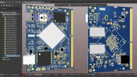
第 7 节:RK3399 的原理图设计,通过网络类对原理图进行引脚映射和阻抗规划。
第 8 部分:Layer Stack up(4/6/8/12L),完成元件布局规划及其执行 Part-1
第 9 部分:组件放置规划及其执行第 2 部分
第 10 部分:组件放置规划及其执行第 3 部分
第 11 节:布局规划、初步布局、高速设计规则和长度匹配、电源平面分段规划、布局优化 Part-1
第 12、13 节:电源平面分段规划,布局优化。
你将学到什么
- 如何从处理器、SDRAM、EMMC、WIFI/BT模块等的需求表中提取选择信息。
- 如何通过定义处理器的核数、缓存、带宽和时钟要求来选择处理器。
- 不同的处理器架构,例如小,大,内存组织。
- 内部和外部SDRAM的类型(DDRX、LPDDRX及其增强版本)。
- DDR5和LPDDR5的外部sdram比较
- SDRAM的不同信号组(数据、地址和命令、控制和时钟组)
- 为移动应用开发一套SDRAM、PMIC、EMMC、WIFI模块、处理器的选择程序。
- 如何阅读RK3399、2GB LPDDR4 SDRAM、16GB EMMC、PMIC、WIFI/BT模块等板中使用的不同组件的数据表。
- SDRAM、EMMC、SDIOs、MIPI、EDPs、Type-C、USB3.0和2.0、SDMMC等的引脚映射,使用RK3399在简单的Excel表上进行。
- 如何使用各自的数据表和设计指南文件设计处理器、SDRAM、EMMC、WIFI、PMIC的原理图。
- 讨论美国、欧洲、加拿大等国的不同WIFI/BT模块认证和监管。
- 在Excel表上绘制1000多个互连的阻抗剖面图。
- 分层叠加(4/6/8/12L),完成元器件布局规划及其执行。
- 布局规划,初步布局,高速设计规则和长度匹配,分段电源平面规划,优化布局回路1和回路2
- FAN-OUT of #828 Balls of RK3399, #200 Balls of LPDDR4 SDRAM and #180 Balls of EMMC.
Genre: eLearning | MP4 | Video: h264, 1280×720 | Audio: AAC, 48.0 KHz
Language: English | Size: 24.8 GB | Duration: 23h 46m
What you’ll learn
How to Extract Selection information from Requirement Sheet for Processor, SDRAMs, EMMC, WIFI/BT modules etc.
How to Choose a Processor by Defining its No. of Core, Cache, Bandwidth, Clock requirements.
Different Architecture of Processor for Ex. Little-big, and Memory Organization.
Types of Internal and External SDRAMs (DDRX, LPDDRX, and their Enhanced versions).
Comparisons of External SDRAMs up-to DDR5 and LPDDR5
Different Signal Groups of SDRAM (Data, Address & command, Control and Clock Groups)
Develop a Set Procedure on selection of SDRAM, PMIC, EMMC, WIFI Module, Processor for Mobile Application.
How to Read the Datasheet of Different components used in this Board RK3399, 2GB LPDDR4 SDRAM, 16GB EMMC, PMIC, WIFI/BT Module etc.
Pin Mapping of SDRAM, EMMC, SDIOs, MIPIs, EDPs, Type-C, USB3.0 & 2.0, SDMMC etc. with RK3399 on a Simple Excel Sheet.
How to Design the Schematic of Processor, SDRAM, EMMC, WIFI, PMIC using their Respective datasheets and Design Guidelines Documents.
Discussion of Different WIFI/BT Module Certification and Regulation as per US, Europe, Canada etc.
Impedance Profile Planning of More than 1000 interconnects on a Excel Sheet.
Layer Stack up (4/6/8/12L), Finish the Components Placement Planning and its Execution.
Layout Planning, Preliminary Layout, High Speed Design Rules and Length Matching, Power Plane Planning by Sections, Optimization of Layout Loop-1 and Loop-2
FAN-OUT of #828 Balls of RK3399, #200 Balls of LPDDR4 SDRAM and #180 Balls of EMMC.
Description
I have Divided this Course into #13 Different Sections Under Each Section You will find Multiple Lessons:
Section 1: Discuss the Requirement sheet and Processor RK3399 Datasheet in very detail.
Section 2: How to Choose a SDRAM (SDR/DDRX/LPDDRX) ? from Very Scratch and Its Pin Mapping and Schematic Design From Datasheet.
Section 3: Selection and Schematic Design of PMIC (Power Management IC) in very Details.
Section 4: EMMC (Embedded Multimedia Card) Chip Selection, Pin Mapping and Schematic Design.
Section 5: WIFI/BT Module Selection, Certification (US/EU/CA), Selection and Schematic Design.
Section 6: Selection of External LDO/DC-DC/Buck-Boost and Their Schematic Design in very Details.
Section 7: Schematic Design of RK3399, Pin Mapping and Impedances Planning on Schematic through Net-Classes.
Section 8: Layer Stack up(4/6/8/12L), Finish the Components Placement Planning and its Execution Part-1
Section 9: Components Placement Planning and its Execution Part-2
Section 10: Components Placement Planning and its Execution Part-3
Section 11: Layout Planning, Preliminary Layout, High Speed Design Rules and Length Matching, Power Plane Planning by Sections, Optimization of Layout Part-1
Section 12, 13: Power Plane Planning by Sections, Optimization of Layout.
Major Schematic Blocks that I have designed in this course are Project Block Diagram, “Power Budget Block Diagram”, “Power Supply Schematic for RK3399”, “PMUIO Schematic Block of RK3399”, “EMMC/PCIE/ADC Schematic for RK3399”, “EDP/MIPI-DSI/HDMI Schematic for RK3399”, “Type-C/USB3.0/USB2.0 Hosts Schematic for RK3399”, “MIPI-CSI/GPIOs/I2C Schematic of RK3399”, “MII/RMII/GMII/RGMII Schematic for RK3399”, “SDR/DDRx/LPDDRx Schematic For RK3399”, “PMIC/DC-DC/LDOs/Buck-Boost for RK3399” and many more various subparts you will learn in this course as you can see on the curriculum sections and their lessons.
You will also Learn some basic hardware designing blocks as well like You will also learn some Basic Blocks as well:
Pre-Schematic Design Blocks (Block Diagram and Power Budget)
Layer Stack-up Selection and Rules for Defining any Stack-up
Different Grounding Techniques( Signal Grounding, Earth Grounding, Chassis Grounding)
Power Distribution Network Analysis (PDN Analysis) of any PCB.
and many more things.
Ferrite Bead, ESD Diodes, and Magnetic Application and their selection.
How to do Placement and Layout Planning on Microsoft-Paint and many more.
After the completion of this course you can design any “Processor Board” without any Simulation models and third party support.
Who this course is for:
People who have Intermediate experience with Hardware design and want to learn it
People Who want to Learn High-Speed Board Design
People who want to learn PCB designing
People who want to Learn How to Select Components out of millions of chip available
People Who wan to Learn How Create a Board on Altium Designer.
People who want to enhance their Electronic Hardware Designing Skills.
People want to Learn Impedance Profile, Length Matching, High-Speed Design Rules, Complex Layout, Advanced Layout Design etc.